SystemVerilog Verification Environment/TestBench for Memory Model
Table of Contents
The steps involved in the verification process are,
- Creation of Verification plan
- Testbench Architecture
- Writing TestBench
Before writing/creating the verification plan need to know about design, so will go through the design specification.
* In this example Design/DUT is Memory Model.
Memory Model Design Specification
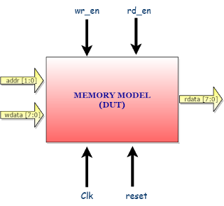
Signal Definition:
| Signal Name | Direction wrt to Design | Description |
|---|---|---|
| clk | input | clock signal |
| reset | input | reset signal |
| addr[1:0] | input | Address signal on which the address is specified |
| wr_en | input | write enable signal, indicates the write operation |
| rd_en | input | read enable signal, indicates the read operation |
| wdata[7:0] | input | wdata signal for write data |
| rdata[7:0] | output | rdata signal for read data |
Operations:
Write Operation:
address, wr_en, and wdata should be driven at the same clock cycle.
Read Operation:
address and rd_en should be driven on the same clock cycle, Design will respond with the data in the next clock cycle.
Design Features,
- The Memory model is capable of storing 8bits of data per address location
- Reset values of each address memory location is ‘hFF
Creation of Verification plan
The verification plan is the list of scenarios need to be verified.
let’s list the few scenarios,
- Write and Read to a particular memory location
- Perform write to any memory location, read from the same memory location, read data should be the same as written data
- Write and Read to all memory locations
- Perform write and read to all the memory locations (as the address is 2bit width the possible address are 2‘b00, 2’b01, 2’b10, and 2’b11)
- Default memory value check
- Check default memory values. (before writing any locations, do read operation we should get default values as ‘hFF)
- Reset in Middle of Write/Read Operation
- Assert reset in between write/read operation and check for default values. (after writing to few locations assert the reset and perform read operation, we should get default memory location value ‘hFF)
TestBench Hierarchy and Architecture
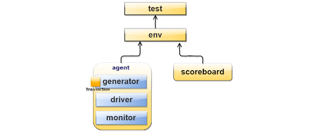
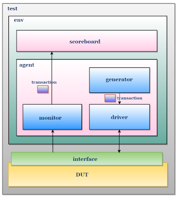
Writing Verification Environment/TestBench
For simplicity will write the two Testbenches,