Let’s Write the SystemVerilog TestBench for the simple design “ADDER”.
Before writing the SystemVerilog TestBench, we will look into the design specification.
ADDER:
Below is the block diagram of ADDER.
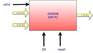
Adder is,
- fed with the inputs clock, reset, a, b and valid.
- has output is c.
The valid signal indicates the valid value on the a and b, On valid signal adder will add the a and b, drives the result in the next clock on c.
Adder add/Sum the 4bit values ‘a’ and ‘b’, and drives the result on c in the next clock.
waveform diagram:
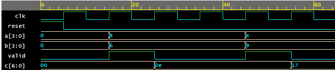
waveform snapshot from EPWave – EDAPlayground
For the simplicity and ease of understanding, let’s write the two TestBecnh’s,